
Quantum Technologies

Today, the quantum revolution is moving beyond research laboratories and becoming part of our everyday lives. Whether it involves designing computers with unprecedented computing power, developing sensors with extreme precision, or securing telecommunications, this transition to industrial-scale applications requires increasingly robust and compact technological building blocks. In this context, photonics is emerging as a key technology for addressing the challenges associated with the development of quantum technologies.
With 20 years of experience, ALPhANOV brings unique expertise gained from related fields to address there major challenges, from designing new fiber-based components and gas cells to developing laser sources at unconventional wavelengths for trapping new cold-atom species.
Beyond individual components, our complex systems engineering combines compact optomechanical design with dedicated electronics development to simplify researchers' work while ensuring maximum performance stability.
Fully committed to helping build and strengthen the quantum supply chain at every level, ALPhANOV is actively involved in the Nouvelle-Aquitaine regional innovation hub Naquidis, develops strategic industrial subsystems through the national AtomQontrol program (France 2030), and contributes to European research consortia through Horizon Europe.
Photonics lies at the heart of emerging quantum applications:

Quantum Computing
Quantum computing architectures (trapped ions, neutral atoms, photonic chip) require highly stable light source, excellent spectral purity, and precise beam control. Photonics plays a key role at various stages, from generating specific wavelengths to routing and distributing them as close as possible to the qubits.
• Precision optical beam conditioning: Laser beam injection, delivery, and shaping systems at the wavelengths required for qubit interrogation, cooling, and manipulation (SOFIA)
• Laser Sources: Amplification and frequency conversion of laser sources to unconventional wavelengths, particularly those corresponding to critical atomic absorption lines, while maintaining high average power and low phase noise (LUMEN, NextWave QPU, GRADIOM projects)
• Highly stable fiber coupling heads: Design of compact fiber arrays to couple and distribute multiple laser sources with high stability, supporting the scaling of quantum architectures and increasing qubits counts (PASQAL, Toptica, QUANDELA, Oxxius, Exail, Max Planck, etc).
Quantum sensing & high-precision metrology
Quantum sensors harness the extreme sensitivity of quantum systems to measure magnetic and electric fields, gravity, and time with exceptional precision. Deploying these sensors outside the laboratory requires miniaturizing and improving the reliability of the optical systems used to interact with atoms.
• Compact light-matter interaction systems: Integration of miniaturized atomic cells and fiber-based light-guiding solutions to reduce the footprint of sensing heads and facilitate system integration (HARMONY, Q-CELL, Cryst^3 projects)
• Robust optical interrogation architectures: Femtosecond laser inscription of optical functions directly into glass substrates to create compact, robust fiber-based systems that are less sensitive to mechanical drift and suitable for harsh environments, particularly in aerospace, space, and defense applications (R&T CNES Photonic Lanterns, RAMEN projects).
NV Center Microscopy
Nitrogen-vacancy (NV) centers in diamond are atomic-scale quantum spin systems that operate at room temperature. Used as nanoscale quantum sensors, they can map magnetic fields, electrical currents, and thermal gradients with exceptional spatial resolution, including within microprocessors and biological structures. Technologies developed for microscopy and security analysis of electronic chip are finding new applications in the design of quantum microscopy platforms. These systems integrate the key functions required for NV-center magnetometry and microscopy: optical control, fluorescence collection, and microwave excitation.
• High-numerical-aperture (NA) fluorescence collection: Engineering of custom optical systems to maximize the extraction and collection of fluorescence photons emitted by NV centers in diamond
• Co-aligned RF and optical excitation: Integration of microwave chips and 532 nm laser excitation paths for high contrast and low noise
• Modular quantum microscopy systems: Wide-field and scanning imaging platforms designed to meet the requirements of R&D laboratories and semiconductor quality control.
Linked collaborative projects
-
LUMEN Project: Visible-emitting fluoride fiber lasers
The LUMEN project brings together academic and industrial partners with the goal of establishing international leadership in the field of high-power (>2 Watts), continuous-wave fiber lasers emitting in the visible spectrum. It aims to address the...
Learn more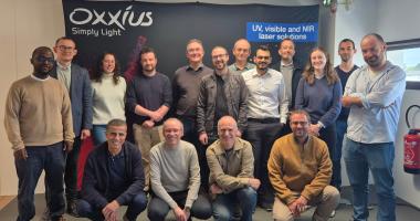
-
Q-CELL - Quantum CELL
Proof-of-concept for a compact, fully fibered rubidium vapor cell.
Learn more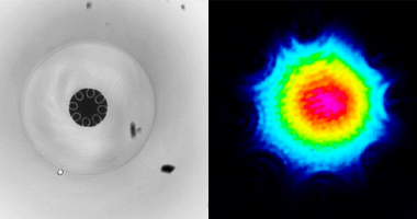
-
CRYST^3 - Prototype of a new material based on individual alkali atoms
Developing a new fully-fiber prototype, based on the trapping and cooling of cold atoms in a hollow core fiber.
Learn more
-
Harmony – Frequency stabilization of lasers using PCF hollow core fibers (HC-PCF)
Develop an all-fiber gas cell component based on PCF hollow core fibers (HC-PCF) that will be used for laser frequency stabilisation.
Learn more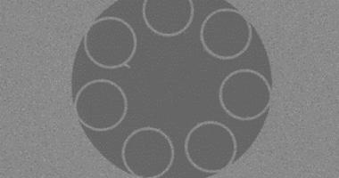
-
Blue laser - Development of blue fiber lasers
(2008 - 2012)
To develop a new family of high-power blue fiber lasers.Learn more


